ADC
// Run Mode Clock Gating Control: base address 0x400F.E000
#define SYSCTL_RCGC2_R          (*((volatile unsigned long *)0x400FE108))
#define SYSCTL_RCGC0_R          (*((volatile unsigned long *)0x400FE100))

// GPIO PortE Registers: (APB) base address 0x4002.4000
#define GPIO_PORTE_DIR_R        (*((volatile unsigned long *)0x40024400))
#define GPIO_PORTE_AFSEL_R      (*((volatile unsigned long *)0x40024420))
#define GPIO_PORTE_DEN_R        (*((volatile unsigned long *)0x4002451C))
#define GPIO_PORTE_AMSEL_R      (*((volatile unsigned long *)0x40024528))

// ADC Registers: ADC0 base address 0x4003.8000	| ADC1 base address 0x4003.9000
#define ADC0_SSPRI_R            (*((volatile unsigned long *)0x40038020))
#define ADC0_ACTSS_R            (*((volatile unsigned long *)0x40038000))
#define ADC0_EMUX_R             (*((volatile unsigned long *)0x40038014))
#define ADC0_SSMUX3_R           (*((volatile unsigned long *)0x400380A0))
#define ADC0_SSCTL3_R           (*((volatile unsigned long *)0x400380A4))
#define ADC0_ACTSS_R            (*((volatile unsigned long *)0x40038000))
System Control Registers Base Address: 0x400F.E000
- System Control Legacy Registers (pg 234)
- RCGC0: 0x100 (pg 454)
- RCGC2: 0x108 (pg 462)
GPIO PORTE (APB) Base Address: 0x4002.4000
- Port Configuration Offsets (pg 657)
- GPIODIR: 0x400 - Direction (pg 660)
- GPIOAFSEL: 0x420 - Alternate Function Select (pg 668)
- GPIODEN: 0x51C - Digital Enable (pg 679)
- GPIOAMSEL: 0x528 - Analog Mode Select (pg 684)
Analog-to-Digital Converter (ADC) base address: ADC0 0x4003.800 & ADC1 0x4003.900
- Port Configuration Offsets (pg 657)
- SSPRI: 0x020 - ADC Sample Sequencer Priority (pg 838)
- ACTSS: 0x000 - ADC Active Sample Sequencer (pg 818)
- EMUX: 0x014 - ADC Event Multiplexer Select (pg 830)
- SSMUX3: 0x0A0 - ADC Sample Sequence Input Multiplexer Select 3 (pg 872)
- SSCTL3: 0x0A4 - ADC Sample Sequence Control 3 (pg 873)
void ADC0_InitSWTriggerSeq3_Ch1(void){ volatile unsigned long delay;
  SYSCTL_RCGC2_R |= 0x00000010;   // 1) activate clock for Port E
  delay = SYSCTL_RCGC2_R;         //    allow time for clock to stabilize

  GPIO_PORTE_DIR_R &= ~0x04;      // 2) make PE2 input
  GPIO_PORTE_AFSEL_R |= 0x04;     // 3) enable alternate function on PE2
  GPIO_PORTE_DEN_R &= ~0x04;      // 4) disable digital I/O on PE2
  GPIO_PORTE_AMSEL_R |= 0x04;     // 5) enable analog function on PE2

  SYSCTL_RCGC0_R |= 0x00010000;   // 6) activate ADC0
  delay = SYSCTL_RCGC2_R;

  SYSCTL_RCGC0_R &= ~0x00000300;  // 7) configure for 125K
  ADC0_SSPRI_R = 0x0123;          // 8) Sequencer 3 is highest priority
  ADC0_ACTSS_R &= ~0x0008;        // 9) disable sample sequencer 3
  ADC0_EMUX_R &= ~0xF000;         // 10) seq3 is software trigger
  ADC0_SSMUX3_R = (ADC0_SSMUX3_R&0xFFFFFFF0)+1; // 11) channel Ain1 (PE2)
  ADC0_SSCTL3_R = 0x0006;         // 12) no TS0 D0, yes IE0 END0
  ADC0_ACTSS_R |= 0x0008;         // 13) enable sample sequencer 3
}-
Step 1: We enable the port clock for the pin that we will be using for the ADC input.
- Set bit 4 to enable the clock for that Port
-
SYSCTL_RCGC0_R |= 0x00010000;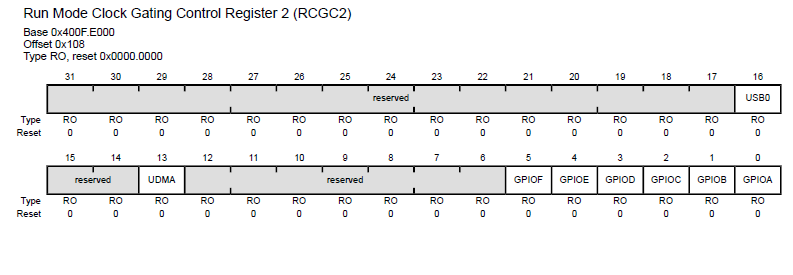
-
Step 2: Make that pin an input by writing zero to the DIR register.
- Clear bit 2 to make that port pin an input data direction
-
GPIO_PORTE_DIR_R &= ~0x04;
-
Step 3: Enable the alternative function on that pin by writing one to the AFSEL register.
- Set bit 2 to enable the alternative function for port pin.
-
GPIO_PORTE_AFSEL_R |= 0x04;
-
Step 4: Disable the digital function on that pin by writing zero to the DEN register.
- Set bit 2 to enable the alternative function for port pin.
-
GPIO_PORTE_AFSEL_R |= 0x04;